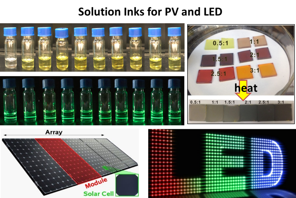
Solution processed perovskite is a new generation thin film technology with solution inks for photovoltaics (PV) and light emitting diode (LED), suitable for application using printing and coating techniques. The world record photoelectric conversion efficiency (PCE) of perovskite-coated PV lies between silicon solar cell (first generation, 26.7%) and thin film solar cell (second generation, ~22%). The luminescent properties, i.e. colour tunability and external quantum efficiency (EQE), of perovskite-based LED are comparable to those of OLED. However, due to its instability, the widespread commercialization of perovskite solar cells is hindered.
We developed a series of ligand-perovskite inks using “non-stoichiometric acid-base reaction (NABR)” that reduce the efficiency-stability-scalability-cost gap of PV/LED devices by half. The inks can be coated on substrates regardless of whether they are rigid or flexible with high throughput. It can be fabricated easily into scalable, flexible and ultrathin films, which is more competitive than nonelastic silicon solar cells. This ligand-perovskite ink technology is promising to be cost-efficiently utilised in the future PV/LED market and would be of great interest to PV/OLED companies as perspective strategies for future development.