Abstract:
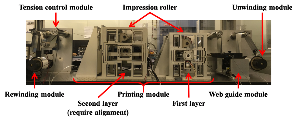
This project aims to develop a scalable precision multi-layer roll-to-roll (R2R) printing system that utilizes a modified Microcontact Printing (MCP) technique to enable high-throughput, low-cost fabrication of submicron-level resolution and registration accuracy photoelectronic devices. Microcontact Printing is a soft lithography technique developed to overcome the diffraction limit; although submicron resolution printing has been repeatedly demonstrated, MCP remains primarily a lab-based technique for academic research and has not been utilized for practical manufacturing. To demonstrate the practicality, this project will deliver R2R fabricated (1) organic field-effect transistor and (2) terahertz metamaterial perfect absorber. To illustrate the capabilities of the high-throughput high-resolution multi-layer R2R manufacturing, we will develop and construct a flexure-based prototype precision multi-layer R2R printing system that demonstrates (1) multi-axis submicron level precision and repeatability, and (2) multi-layer submicron level registration accuracy. The flexure mechanisms, i.e. compliant mechanisms, have been used extensively in many lithography alignment systems and proved to substantially improve the printing repeatability, accuracy, and resolution. The developed technology could be widely adapted to manufacture low cost photoelectronic devices.
Problem to be solved:
1: Design and construct a multi-axis flexure guided R2R system
2: Develop a multi-layer flexure-based R2R printing system
3: Develop process to fabricate submicron resolution samples using MCP
4: Design and optimize fabrication parameters for printable optical gratings and metal grids
5: Design and implement a submicron accuracy multi-layer registration method
6: Incorporation of MCP metal grids into flexible organic photovoltaic cells
Applications:
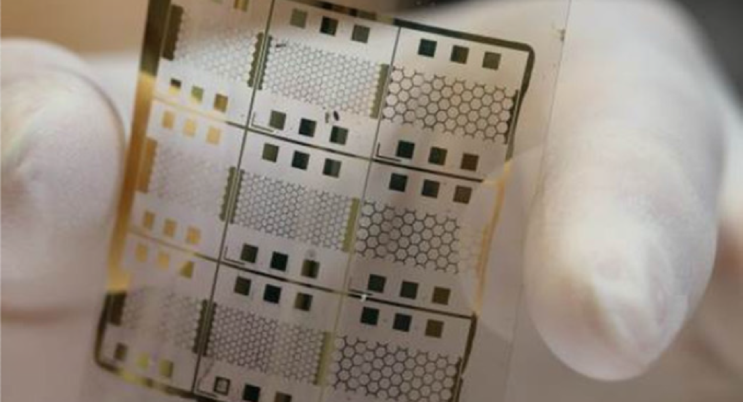
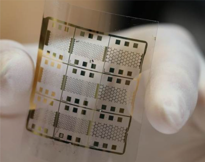
1: diffraction gratings
2: high resolution ~85% transparent metal grids
3: flexible organic photovoltaic cells that utilize the metal grids as electrodes
4: organic thin-film field-effect transistor
5: photonic metamaterial, e.g. terahertz perfect absorber
6: multi-layer flexible printed circuit
Target Users:
Manufacturers of flexible electronics/ photoelectronic devices