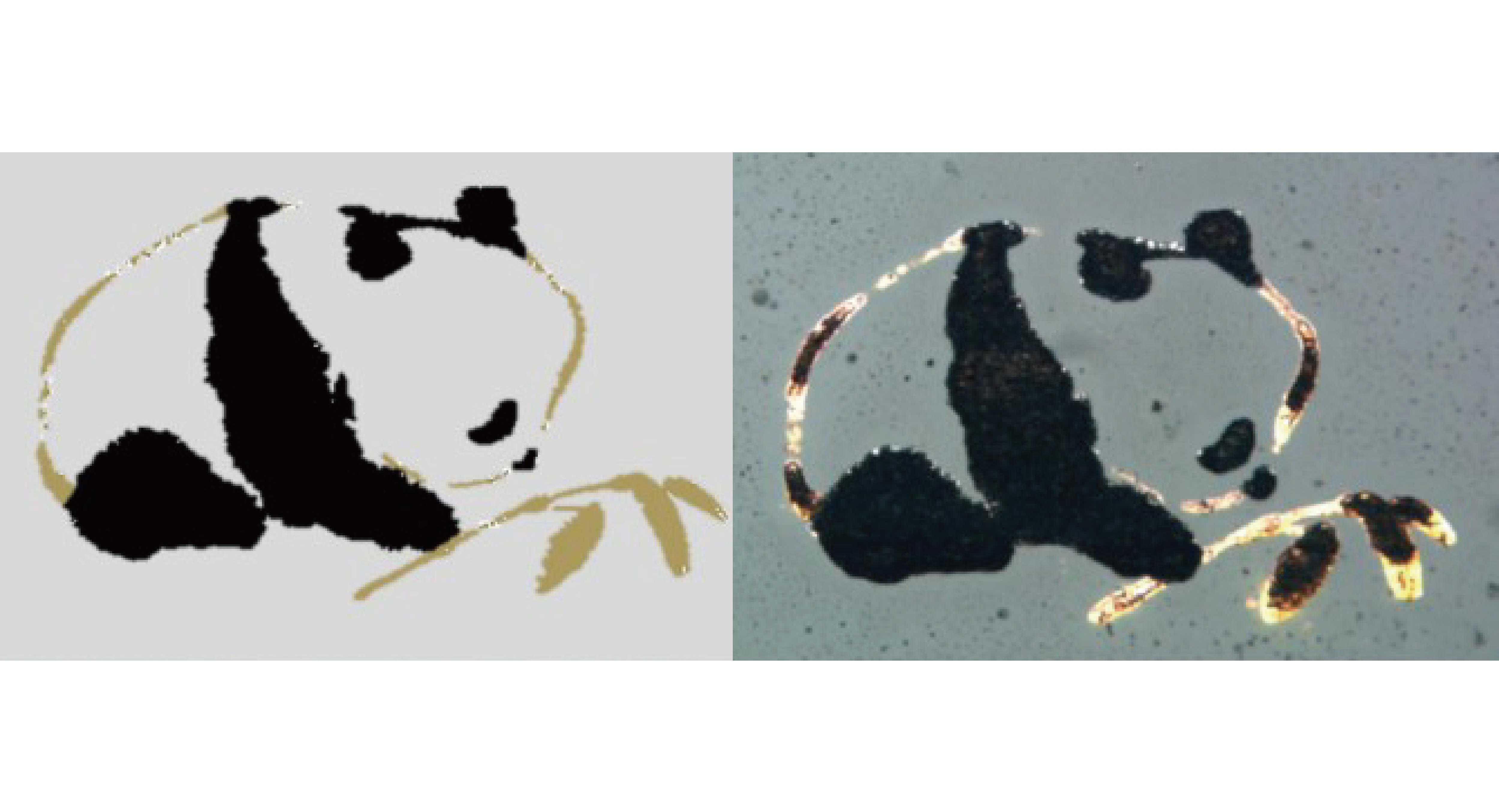
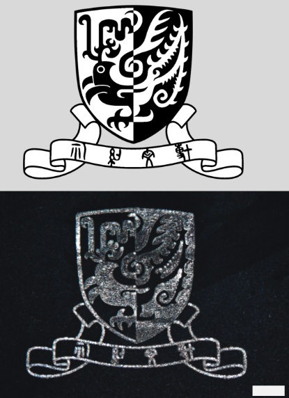
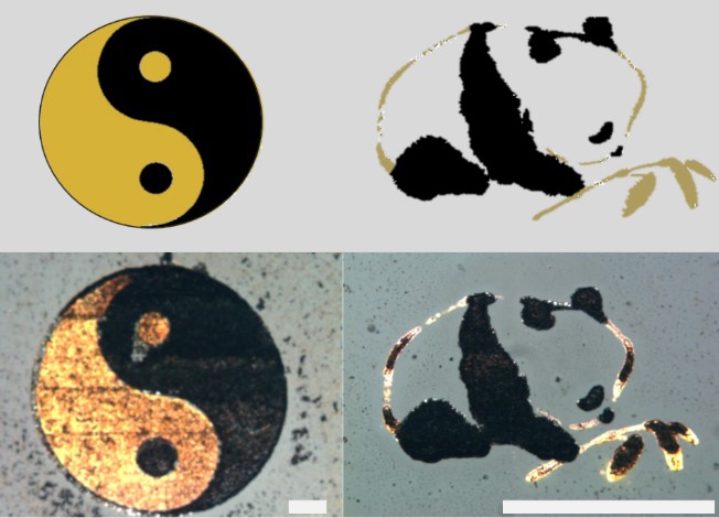
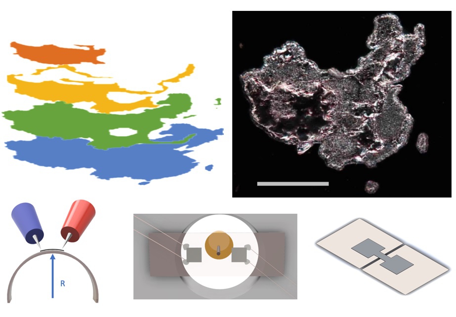
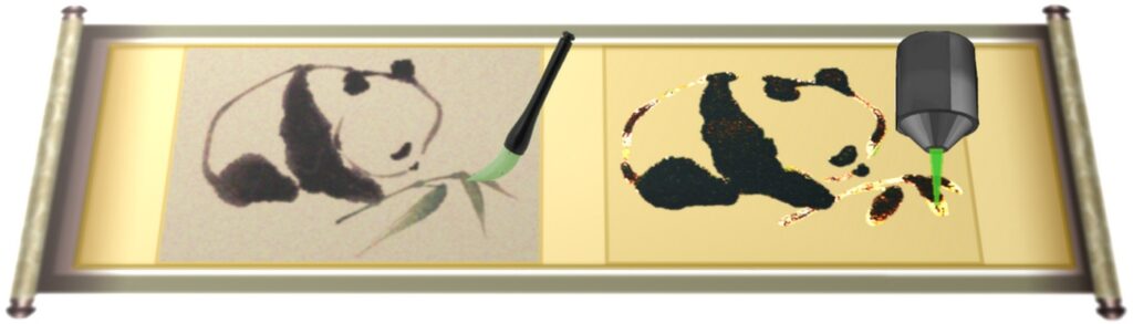
Stemming from fundamental physics principles, the research team came up with a brand-new idea for material deposition. They combined the optical tweezer technique and semiconductor photoelectric effect, by introducing semiconductor nanoparticles suspension into metallate solution to form the “universal ink”. The focused laser beam triggers both effects simultaneously and induces chemical reduction reactions on the nanoparticles. The reduced metal particles accumulated on the semiconductor nanoparticles work as “glue” to join each other into a solid structure and attach to the substrate. By changing the focus position, selective deposition at an arbitrary position on the substrate is achieved. Through the change of “ink” recipes, the team realized deposition with various materials on different substrates.