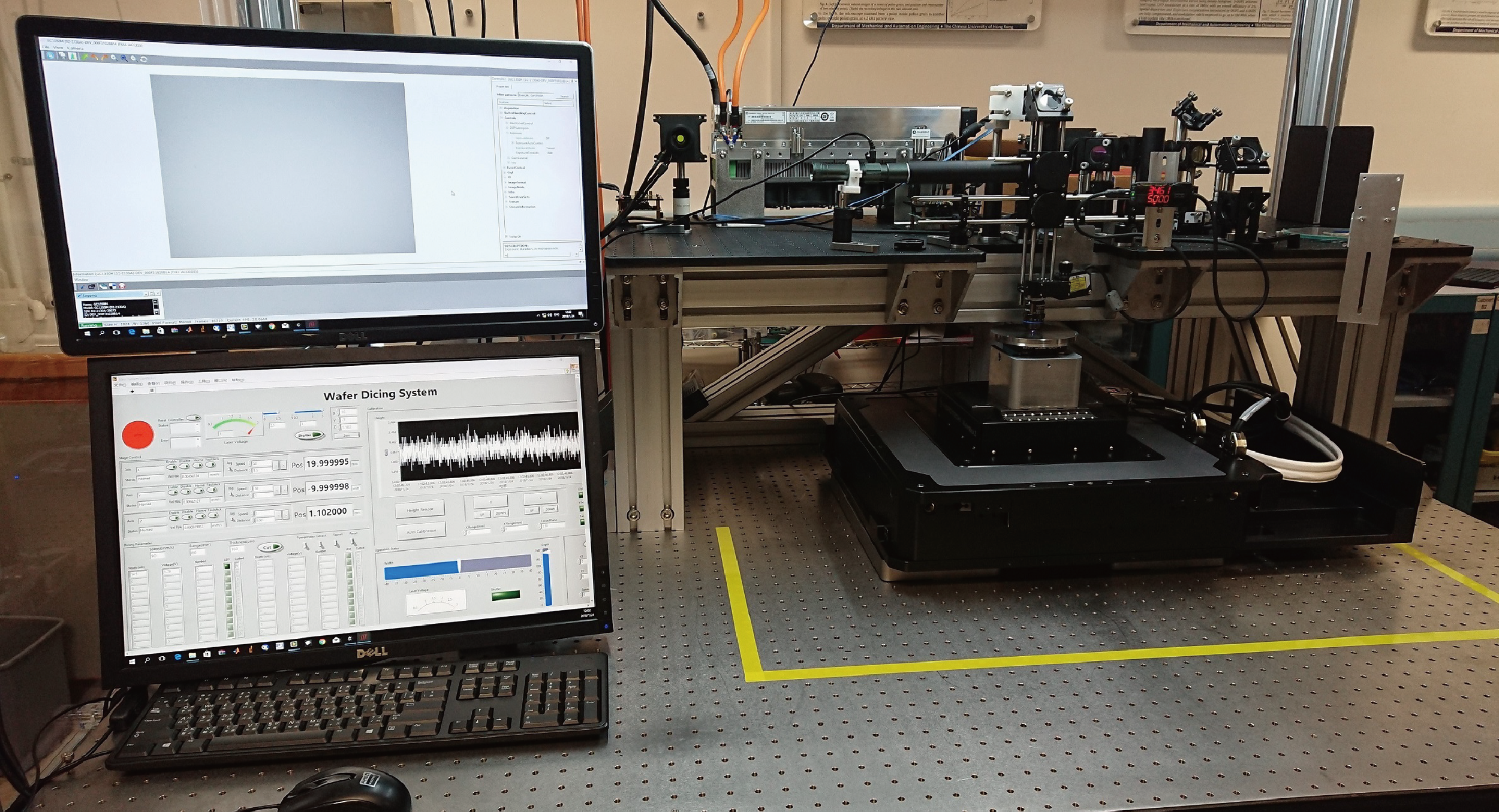
High-efficiency stealth laser dicing system for semiconductor wafer
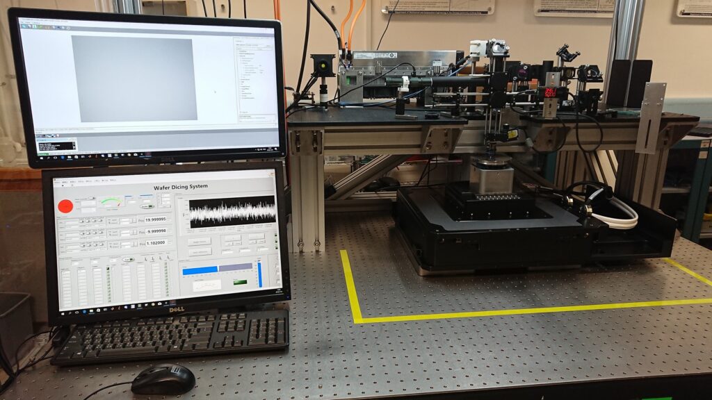
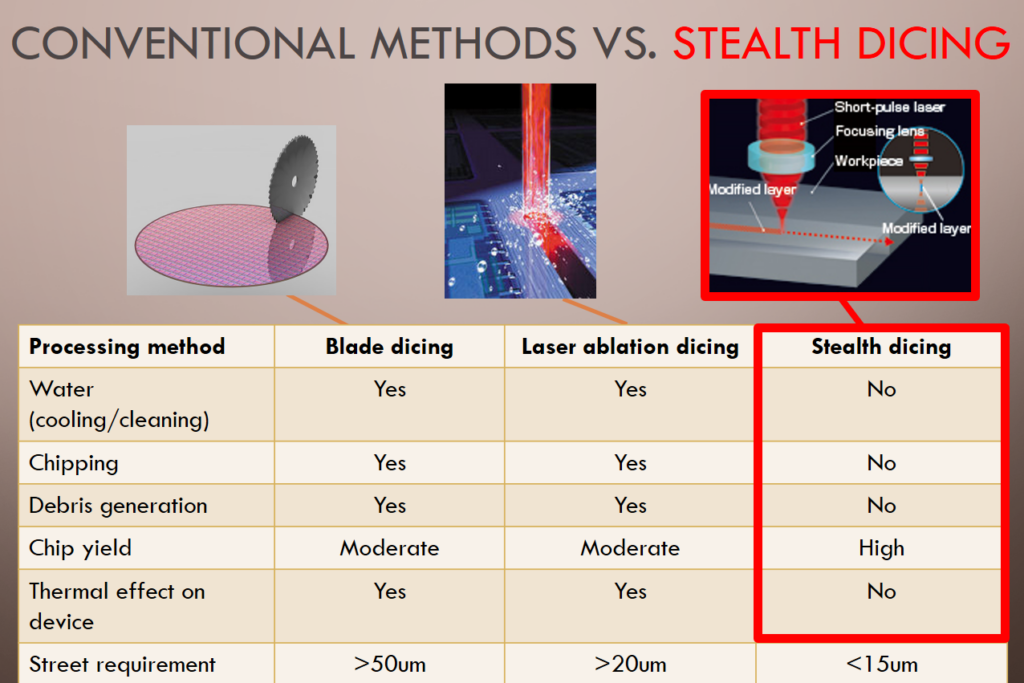
Conventionally, semiconductor wafer dicing is performed by blade dicing or laser ablation dicing, where materials are mechanically removed or pulverized in the cutting path, causing issues such as debris, contaminations, or damage to the devices etc. CUHK research team develops a new high-speed stealth laser dicing (SLD) system for processing wafer based on simultaneous application of pulsed Bessel beams at different depths of a wafer. SLD refers to a process that utilizes a laser beam to introduce defects inside a semiconductor wafer for separating it into many small pieces with better resolution, higher precision and speed. Moreover, enhanced process compatibility, and minimized contamination and damage to the wafer are also the advantages.
Why Bessel beam?
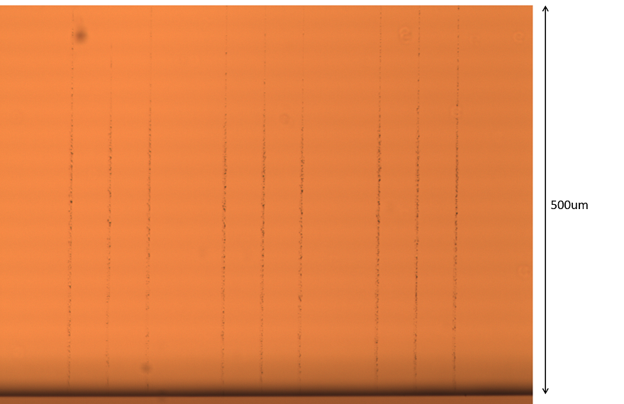
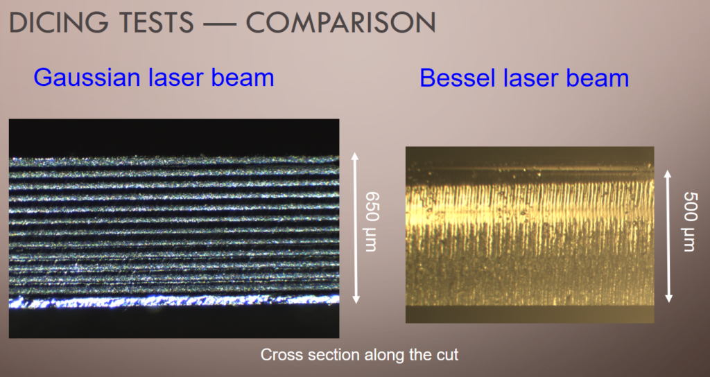
Bessel beam is a “non-diffracting” beam, where its transverse intensity profile does not vary as it propagates, making it the ideal laser beam to perform laser cutting. We applied multiple Bessel beams to perform the laser dicing process in parallel, achieving higher throughput with both nanosecond and femtosecond lasers. With the new beam, the SLD modified layer is many times thicker by one pass.
Applications:
Laser cutting; Wafer dicing; Sapphire grooving; Die cutting; MEMS fabrication
Target Users:
Semiconductor devices/chip manufactures
