This project aims to develop a light-guided metal-assisted chemical etching system. It utilizes metal nanoparticles as a catalyst to generate positive charges (i.e., holes) through local band bending. Combined with UV light excitation, high energy holes can be generated, thus facilitating the etching process. By fine tuning the light direction, intensity and exposure time, as well as selecting the proper geometry and type of the metal nanoparticles, we can precisely control the position, velocity and direction of the etching reaction. Through the holistic efforts of system development, recipe optimization and theoretical modeling, the project will deliver both the hardware designs and well-established processing protocols for high-throughput fabrication of three-dimensional micro- and nano- structures required for new generation 3D IC chips.
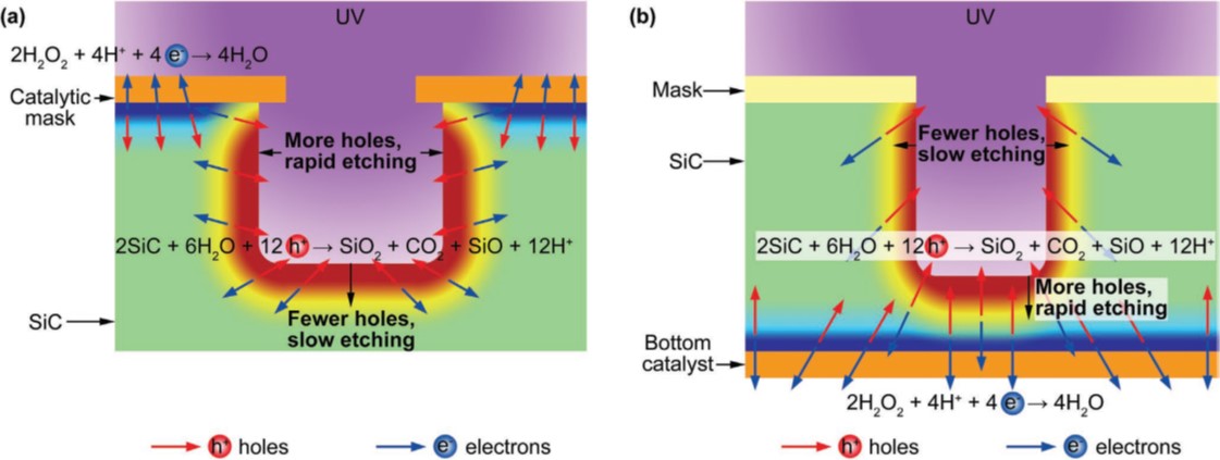
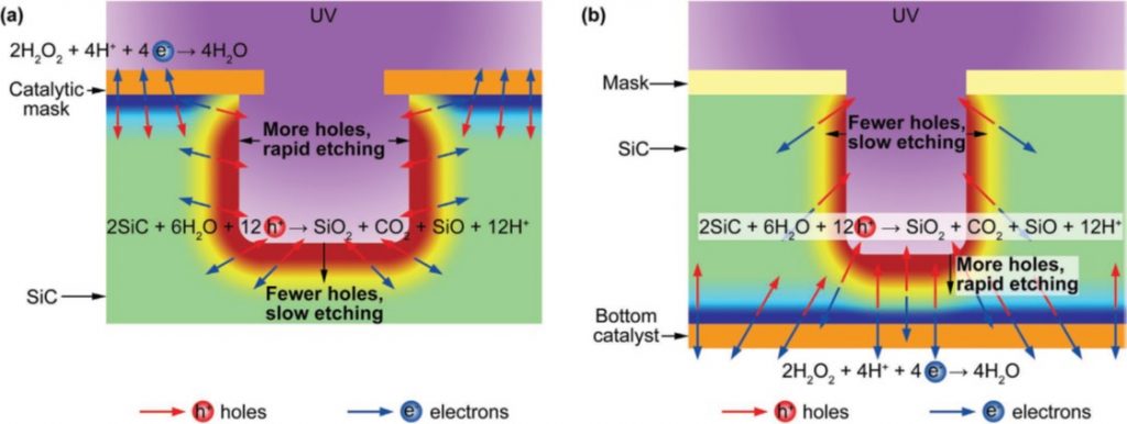
Schematic illustration of a) a common photo-electrochemical etching method for SiC wafers and b) our proposed anisotropic charge transport directed etching structure
Uniqueness and Competitive Advantages:
Can fabricate complex bended structures with controlled position, velocity and direction of the etching reaction
Compact hardware designs and well-established processing protocols are useful for high-throughput fabrication of three-dimensional micro- and nano- structures